
MIRTEC GENESYS-CC: Killing the Shadow Zone in Coating Inspection
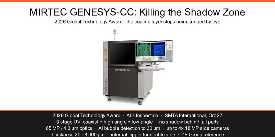
MIRTEC GENESYS-CC: Killing the Shadow Zone in Coating Inspection
An SMT line has three inspection checkpoints it trusts completely: SPI watches the paste, AOI watches the placement, AXI watches the solder. Then the board goes through the coater, and the fourth and final layer — the one that decides whether the assembly survives five years of humidity, salt fog and thermal cycling — is still checked with a UV lamp and a trained pair of eyes.
That gap is what the MIRTEC GENESYS-CC was built to close, and on October 27 the industry said so out loud: at the SMTA International exhibition in Rosemont, Illinois, the system took the 2026 Global Technology Award in the AOI Inspection Systems category. Not “coating equipment” — AOI. That category shift is the actual headline.
Why coating has been the blind spot
Conformal coating inspection is hard for structural reasons, not for lack of effort:
- UV fluorescence tells you whether there is coating, not how well it is applied. Acrylic and silicone chemistries fluoresce differently, so a single lighting recipe under-reports on one of them.
- Tall parts cast shadows. A UV ring firing from one angle leaves the lee side of every electrolytic can, connector body and shield frame dark. Dark reads as “not coated”, the operator clears it, and a real void walks out the door with a signature on it.
- Top-down optics cannot see the sides. J-leads, connector sidewalls and the flanks of chip components are exactly where coating wicks, splatters, bubbles and cracks — and exactly where a vertical camera has no line of sight.
- Bubbles live below the resolution of a general-purpose AOI. A 100 µm bubble under a 60 µm coating is a moisture path, not a cosmetic defect.
Put together, the industry settled for sampling: coat, cure, pull a few boards, look under UV, ship. On automotive and medical boards that is a statistical bet, and the loss shows up two years later as field corrosion.
The innovation: three UV angles instead of one
GENESYS-CC’s answer to the shadow problem is a 3-stage UV illumination system that fires from three distinct geometries:
- Coaxial UV — light on the optical axis, which suppresses specular glare off glossy coating and separates a thin film from a bare laminate.
- Vertical (high-angle) UV — fills the floor of the pocket between tall components.
- Angled (low-angle) UV — grazes the surface at a shallow angle so a missing film shows as a hard edge instead of a soft gradient.
MIRTEC’s own comparison frames it well: with one stage you get shadow and weak signal; with three stages the same field renders as a clean, high-contrast coating map. Because the recipes are switchable, the same machine can be tuned for acrylic and for silicone without a hardware change — which is the difference between a system that inspects your process and one that inspects a process.
Side cameras: the view that was never available
A top-down AOI, however good, is a 2.5D instrument. GENESYS-CC adds up to four 18 MP side-angle cameras for lateral inspection — component sides, connector bodies, J-leads and solder joints — where the real defect vocabulary lives: uncoated flanks, splatter on keep-out areas, bubbles trapped against a lead, hairline cracks in the film.
The primary imaging chain is MIRTEC’s 15 MP CoaxPress camera technology, with the optical system configurable up to 65 MP at 4.3 µm resolution. That resolution is not a spec-sheet ornament; it drives the detection floor directly.
The number that matters: 30 µm
MIRTEC publishes the relationship between sensor, lens and the smallest bubble the system can resolve:
| Camera | Lens resolution | Smallest detectable bubble |
| 15 MP | 15 µm | 100 µm |
| 25 MP | 7.2 µm | 48 µm |
| 50 MP | 4 µm | 30 µm |
At the top of that range the platform reaches 30 µm micro-bubble detection, and the algorithm behind it is AI-driven — it keeps improving as it learns from production images rather than staying frozen at the day of installation. For a coater running 25–75 µm films, 30 µm is the point where a bubble stops being a cosmetic question and becomes an electrical-reliability one.
Two more things that change the process
Coating thickness as a measurement, not an inference. An optional sensor measures transparent film thickness from 20 µm to 8,000 µm depending on configuration, on both component tops and bare board. That converts “coverage percentage” — a number that hides everything — into an actual film-thickness distribution you can put on an SPC chart.
A flipper built into the conveyor. Double-sided assemblies normally mean either two passes on two machines or an external handler bolted onto the line. GENESYS-CC carries an internal PCB flipper, so top and bottom are inspected in one machine without buying floor space twice. That is an integration decision as much as an engineering one.
The commercial proof point
In January 2026, ZF Group — one of the largest automotive Tier 1 suppliers in the world — partnered with MIRTEC specifically for advanced conformal coating inspection. Automotive is the harshest possible validation ground for this class of equipment: the qualification cycle is long, the audit trail is brutal, and a coating escape is a warranty event rather than a rework ticket.
When an AOI vendor wins an award in the AOI category for a coating machine, and a Tier 1 signs on, the signal is that coating inspection has moved from the “audit” column into the “process control” column.
Five questions before you spec one
- What is your actual film thickness? Ask for the bubble-detection table for the lens you are buying, not the headline. If you run 30 µm films, a 100 µm detection floor is not adequate.
- Which chemistries run on your line? Acrylic, silicone, polyurethane and parylene behave differently under UV. Confirm the illumination recipes exist for each, and ask for sample images from your own material.
- Where are your escapes coming from? Shadow behind tall parts, side-of-lead voids, splatter, and bubbles demand different optics. The 3-stage UV and the side cameras solve different problems — make sure you are buying the one your defect Pareto points at.
- Do you need the flipper? If more than a third of your volume is double-sided, the internal flipper changes both footprint and takt. If not, spend the budget on resolution.
- How does the data leave the machine? Coating thickness and defect maps are only useful if they reach your SPC or MES. Confirm the interface and the traceability format before installation, not after.
The bottom line
Every other inspection step on an SMT line has already been industrialized — paste volume, placement offset, solder void. Coating was the last one still argued over with a UV torch and a judgment call. GENESYS-CC is interesting less because it is a better camera than because it moves the whole question from look to measure: three UV geometries to remove the shadow, side cameras to see the flanks, 30 µm resolution to catch the bubble, and a thickness sensor to put a number on the film.
That is what an innovation in inspection actually looks like — not a faster way to make the same decision, but a way to stop making it by eye.