
Koh Young ZenStar: True 3D Inspection Moves to the Wafer
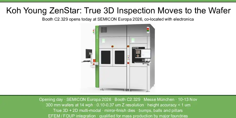
Opening day, Messe München. This morning the doors open on electronica 2026 — and on SEMICON Europa 2026, the semiconductor show co-located in the same halls from 10–13 November. On the semiconductor side of the fairground, at Booth C2.329, Koh Young is making a statement about where inspection goes next: upstream, to the wafer itself.
The incumbent, looking beyond the board
Koh Young has been the market leader in True 3D inspection since 2006, and its SPI and AOI systems anchor thousands of SMT lines. That is exactly why its SEMICON Europa announcement deserves attention from SMT buyers: the company is not chasing a new camera, it is moving its measurement franchise to where its customers’ hardest problems now live — advanced packaging and wafer-level processing.
The two systems on Booth C2.329 frame that move. ZenStar handles wafer-level inspection and metrology; Meister D+ covers the singulated die. Together they span the steps between the fab and the SMT line — the zone where chiplets, 2.5D stacks and fan-out packages are making “board-level quality” a wafer-level question.
True 3D Inspection ZenStar: the numbers that matter
The ZenStar is a production machine, not a lab brochure. Its core specification:
- 300 mm wafers at 14 wafers per hour — roughly 450,000 bumps, balls and components per wafer, the volume that makes sampled measurement impractical
- Z resolution 0.10–0.37 µm with height accuracy under 1 µm (±1.5 % at 300 µm), maximum inspection height 500 µm
- Camera options: 12 megapixel at 5 µm or 25 megapixel at 3.5 µm XY resolution
- True 3D + 2D multi-modal: Moiré measurement plus proprietary optics, engineered for mirror-finish, highly reflective dies that defeat conventional optics
- AI deep learning for micro-cracks, chipping and foreign material
- Cleanroom integration: rated Class 1000 / ISO 6, with EFEM and FOUP support, ring-frame wafer handling with multiple load ports and a dual-arm robot, and a stable multi-hole vacuum chuck
Koh Young states the ZenStar has been qualified for mass production by major semiconductor foundries — the point that separates this announcement from concept-stage wafer inspection tools.
Metrology, not just inspection
The framing Koh Young brings to Munich is worth quoting: inspection answers a binary question — pass or fail. Metrology answers a quantitative one — how tall, how flat, how much volume, by how many microns. In advanced packaging, where the margin between a good joint and a reliability risk is measured in single-digit microns, that difference decides whether you can control a process or only sort its output.
That is also why the story resonates for SMT engineers. The same logic Koh Young built its SPI business on — measure the deposit, feed the number back to the process — now runs one level up: bump geometry at the wafer, die tilt after placement, paste volume on the substrate. Measurement data from each stage feeds KSMART, so a drift detected at one step can be traced to the process step that caused it.
Meister D+ keeps the die honest
Beside the ZenStar, the Meister D+ extends Koh Young’s Moiré-based measurement to singulated dies: height, tilt, coplanarity and position on mirror-finish surfaces, with small-die and narrow-gap inspection down to 50 µm, and defect detection for micro-cracks, chipping and foreign material. For factories assembling SiP, MCM, chiplet modules and interposer-based packages, it is the bridge between wafer-level metrology and final-board AOI.
Five questions to ask at Booth C2.329
A fair-week visit is worth more with pointed questions:
- Throughput in practice — what does 14 wafers per hour look like on a mixed product mix, not a golden wafer?
- Which camera config for which package — when does 25 MP / 3.5 µm justify itself over 12 MP / 5 µm?
- Reflection limits — what die finishes and materials still fall outside the mirror-surface guarantee?
- Fab integration — how complete are the OHT and SECS/GEM options in current shipments?
- The path back to the line — how does ZenStar measurement data join KSMART feedback into SMT printing and placement?
Why today matters
Electronica has always been where the electronics industry takes stock. This year, the co-location with SEMICON Europa makes the message sharper: the boundary between SMT and semiconductor packaging is dissolving, and the inspection leaders are moving first. Koh Young, the company that made 3D measurement the standard on the SMT line, is now applying the same discipline one step earlier — to the wafer that feeds the line.