
Koh Young Meister D+: True 3D Inspection Steps Up to Mirror-Finish Dies
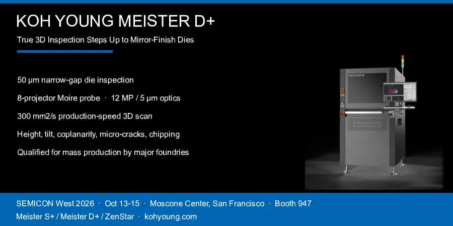
Innovation spotlight — Koh Young Technology, ahead of SEMICON West 2026 (October 13–15, Moscone Center, San Francisco, Booth 947)
Every SMT engineer knows Koh Young as the company that made 3D solder paste inspection standard equipment. Since pioneering the first 3D SPI system with dual-projection Moiré technology in 2002, the Korean firm has held the world’s No. 1 position in SPI and AOI. Now it is taking the same True3D measurement foundation somewhere far harder: inside the semiconductor back-end, where the parts you need to inspect literally shine light back at you.
The mirror problem
As phones and AI accelerators demand thinner packages, dies must be thinned — and a thinned die becomes a mirror. Highly reflective, polished silicon surfaces return unusable data from conventional optical projection, which is precisely why die-level 3D inspection has been a long-standing challenge for the industry. Add tighter inter-die spacing, higher aspect ratios, and micro-cracks or chipping that hide in a few microns of relief, and traditional pass/fail vision simply gives up.
The Meister D+ is Koh Young’s answer. It pairs the company’s industry-leading Moiré measurement technology with new proprietary optics engineered specifically for mirror-finish dies, delivering full 3D height, tilt, coplanarity, and position measurement where conventional projection returns noise. An 8-projector probe with 12-megapixel, 5-micron optics scans at up to 300 mm² per second — production speed, not laboratory speed.
What it actually measures
- Small die and narrow gaps: inspection down to 50 µm gap spacing, plus 0201M (008004) microchips, 10 µm bump heights, and 5 µm gap features
- True defect detection: micro-cracks, chipping, and foreign material — not just “is the die present,” but dimensional data that tells engineers how well it was placed
- Missing, offset, rotation, polarity and full dimension/co-planarity checks in one platform
- AI-assisted analysis with built-in measurement and defect software, plus programming wizards that virtually eliminate fine-tuning and teaching
- Standard connectivity: IPC-CFX-2591, IPC-HERMES-9852, and IPC-DPMX-2581
The approach has already been qualified for mass production by major semiconductor foundries and Mini/Micro-LED manufacturers — the strongest signal that this is production tooling, not a concept demo.
One measurement foundation, many platforms
At SEMICON West, Koh Young will display the fuller picture: the Meister S+ for micro solder and flux deposition (including transparent flux, a nightmare for conventional optics, with enhanced warpage compensation), the Meister D+ for die inspection, and ZenStar for wafer-level 2D/3D metrology with EFEM and FOUP integration and the high-resolution Zeta probe pushing beyond traditional micro-bump sizes.
“Advanced packaging is becoming a multi-platform market, and we do not expect one inspection configuration to solve every application,” says Joel Scutchfield, General Manager of Koh Young America. “Our approach is to start with the same foundation of accurate 3D measurement and then apply the optics, resolution, algorithms, and handling the application requires.”
That is the real innovation here. SiP, flip-chip, fan-out, panel-level, and wafer-level packaging are converging on the same production floors as classic SMT — and the inspection strategy that treats measurement as process control rather than end-of-line gatekeeping is moving with them. If you are at SEMICON West 2026, Booth 947 is worth the walk.